How to Draw Electrical Schematics and Generate a Live BOM in Your Browser
Step-by-step tutorial: open Electrical mode, place passive and IC symbols, enter SI shorthand values, connect pins with Manhattan auto-routing, trace nets, and export a live Bill of Materials.
TLDR
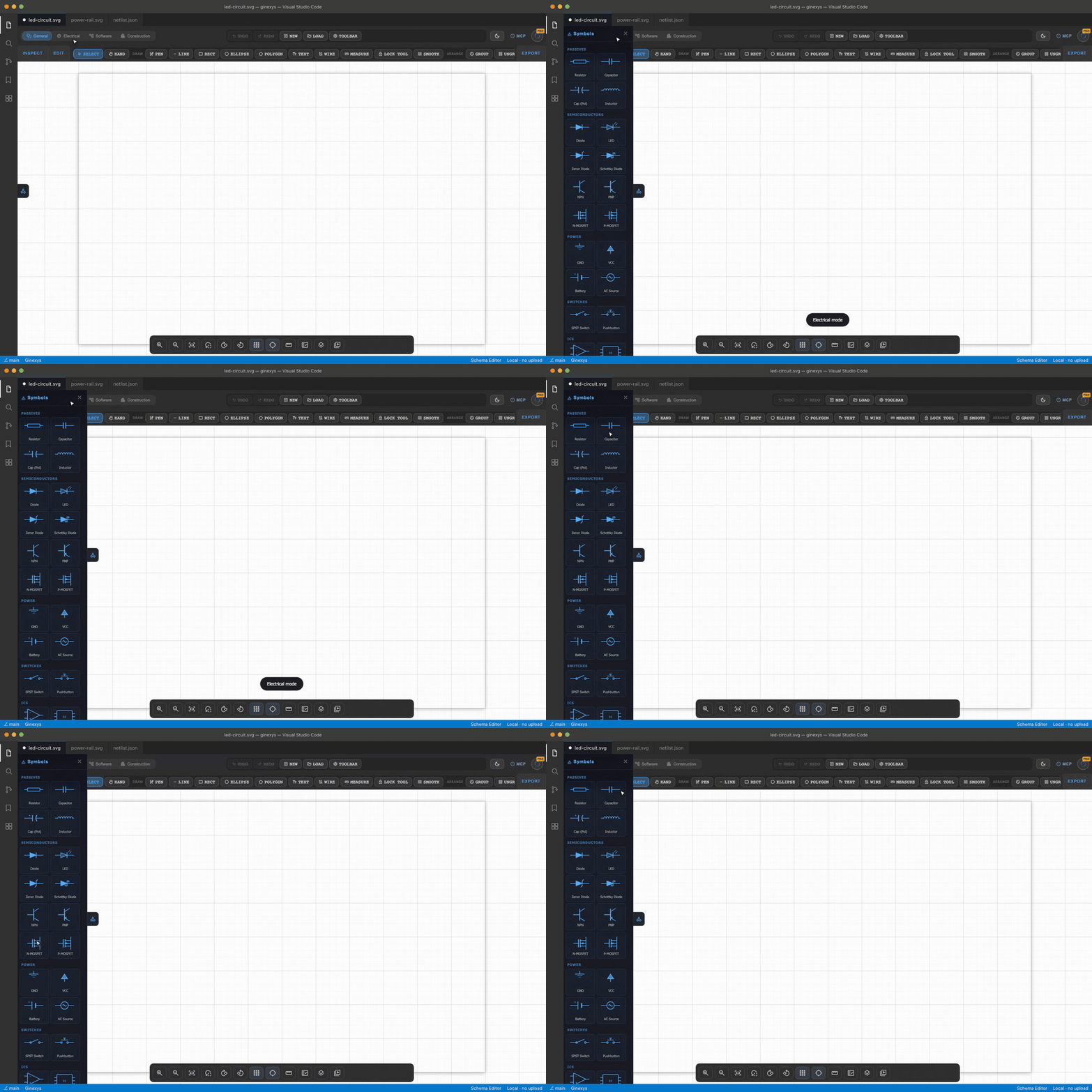
Open Schema Editor in Electrical Mode, drag standard schematic symbols (resistors, capacitors, ICs) onto the canvas, and enter engineering values using standard shorthand like 4k7 or 100n. Click between component pins to route clean 90° wires with automatic obstacle avoidance, verify signal connectivity using Trace Mode, and click Generate BOM to compile a complete parts list sent directly to Table Formatter.
Before you start
You need a web browser and your circuit design concept. Schema Editor runs entirely client-side, saving SVG schematics and component attributes locally without requiring multi-gigabyte desktop EDA installations.
Step 1 — Open Schema Editor in Electrical mode
Navigate to Schema Editor and select Electrical Mode from the top mode selector (or load /tools/schema-editor/electrical/).
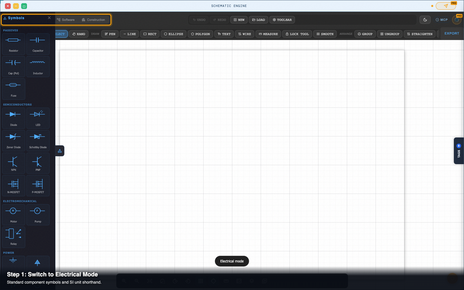
The workspace displays an engineering grid canvas, a component symbol palette on the left, and a properties inspection panel on the right.
Step 2 — Place components from the symbol library
In the left-hand symbol palette, click on any component category:
- Passives: Resistors (
R), Capacitors (C), Inductors (L), and Diodes (D). - Power & Ground:
VCC,GND,+5V,+3.3V. - Active ICs: Op-amps (e.g.
LM358), Microcontrollers (e.g.ATmega128), and Logic Gates.
Step 3 — Enter component values with SI shorthand
Click on any placed component (such as R1 or C1) to open the Properties Panel on the right.
Type standard engineering shorthand into the Value field:
4k7automatically resolves to4.7 kΩ.100nautomatically resolves to100 nF.2u2automatically resolves to2.2 µF.1Mautomatically resolves to1 MΩ.
Step 4 — Wire pins with orthogonal Manhattan routing
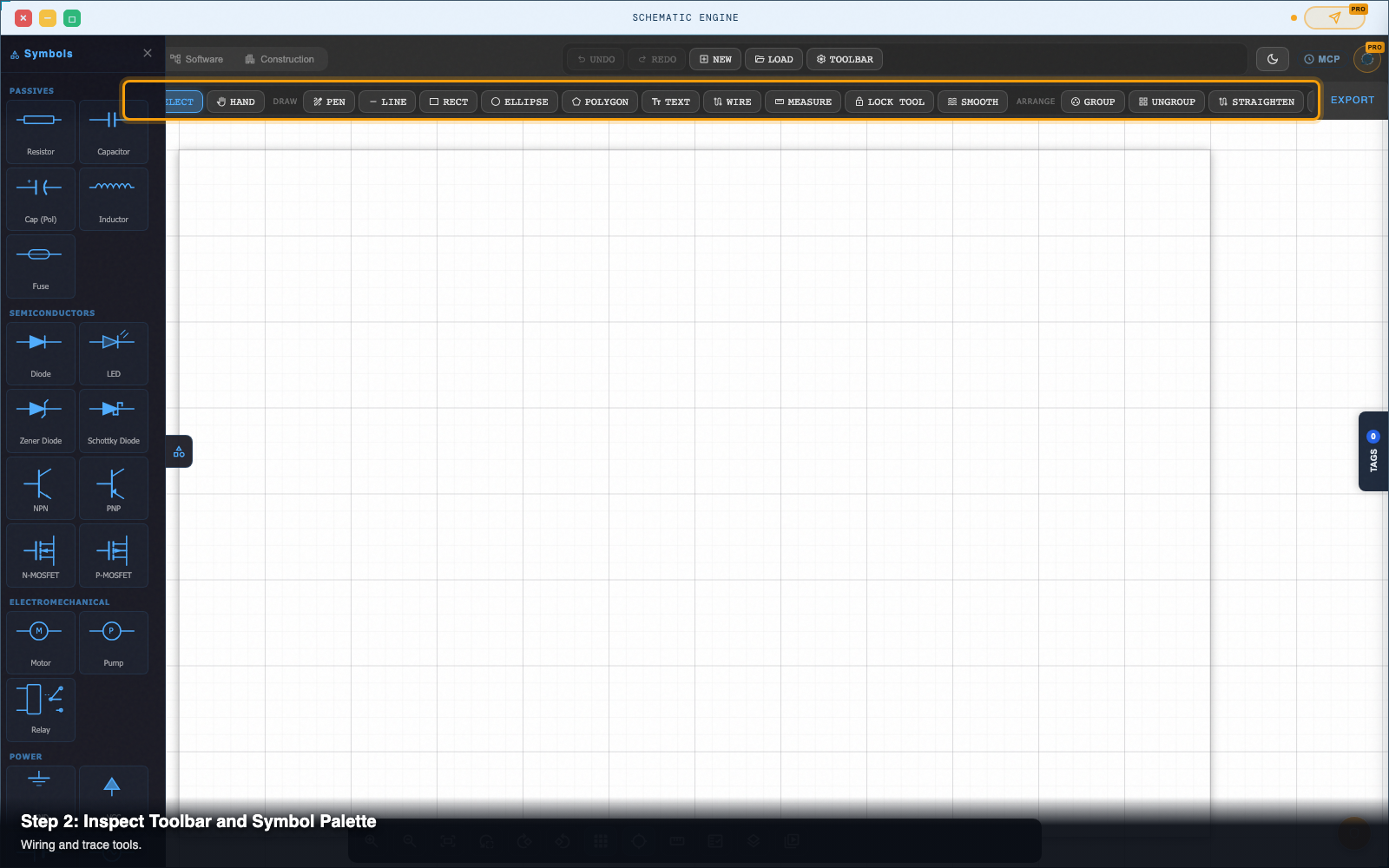
Click on a component terminal pin (highlighted with a green node marker).
- Move your cursor toward the destination pin.
- The router automatically draws a clean 90° orthogonal wire path that steers around other components on the canvas.
- Click the target pin to complete the connection. A junction dot automatically renders where three or more wires meet.
Step 5 — Inspect connections with Net Trace mode
Click Trace Mode in the top canvas toolbar (or press T).
Click any wire segment or component pin:
- The entire electrically connected net illuminates in bright green across your schematic.
- Isolated pins and unconnected floating nets remain dim, helping you catch missed connections instantly before building your board.
Step 6 — Click Generate BOM to export a parts list
In the top action bar, click Generate BOM (Bill of Materials).
Schema Editor aggregates all canvas components, groups identical values by footprint and reference designator, and packages the parts list:
- Send to Table Formatter: Dispatches the tabular parts table directly into Table Formatter over local OS IPC for pricing and procurement analysis.
- Export CSV / JSON: Downloads the structured BOM ready for upload to component distributors like DigiKey, Mouser, or JLCPCB.
Pro tip: SI unit auto-normalization
When generating a BOM, entering 4700 for one resistor and 4.7k for another often causes traditional spreadsheets to treat them as two different line items.
GINEXYS Schema Editor normalizes all component values to standard SI base units behind the scenes, ensuring that 4k7, 4.7k, and 4700 group into a single consolidated line item with an exact quantity count.
Next steps
Schema Editor — Draw and edit wiring diagrams, schematics, ERDs, and state machines as real SVG.